Real-space visualization of atomic- and molecular-scale structures has always attracted researchers, and they welcomed the invention of scanning tunneling microscopy (STM) in 1981. STM images of many crystalline compounds revealed their atomic and molecular arrangements as well as various single-atom defects. STM applications, however, were limited due to requirement of sample conductivity.
Therefore, Atomic Force Microscopy (AFM), which can be applied to any kind of sample, became the leading scanning probe method. For the past 20 years AFM has been developed into a powerful characterization technique but the question of atomic-resolution in AFM is still open. The initial AFM measurements were performed in contact mode and atomic-scale lattices were first revealed in the images of graphite, MoS2, boron nitride and mica [1]. Similar observations were later reported for a large number of organic and inorganic crystals and layers [2]. These images were usually obtained using Si3N4 AFM probes (average AFM tip size ~20nm) and soft silicon AFM probes (AFM tip size in the 10-20nm range).
The main drawback of these images was the absence of atomic-scale defects, which implies only lattice but not true atomic resolution [3]. The latter suggests a presence of single-molecular defects that, indeed, were observed in AFM images obtained in oscillatory frequency modulation (FM) and amplitude modulation (AM) modes. The images of surface lattices of Si (7x7) and InP crystals were obtained in FM studies in UHV [4-5]. Later, true atomic-scale FM visualization of mica and polydiacetylene (PDA) crystals was achieved in air and in water [6-8].
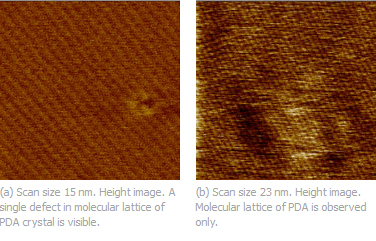
| Fig. 1. (a) Height image of polydiacetylene crystal obtained with Dimension 5000 SPM microscope and Hi'Res-C AFM probe; (b) Topography image of polydiacetylene crystal obtained with Agilent 5500 SPM microscope and HQ:NSC14 AFM probe. Image courtesy of Dr. S. Magonov (Agilent). |
 |
These results were obtained by researchers who used custom instruments with optical deflection and interferometric detection systems. It also became clear that FM is not a unique oscillatory mode for observation of surface lattices with defects and similar results were achieved in AM studies in air [9-10]. The related images of polydiacetylene crystal obtained with Dimension 5000 (Bruker) and Agilent 5500 (Agilent Technologies) microscopes, Fig. 1. In these studies different MikroMasch AFM probes such as Hi'Res-C and HQ:NSC14 were used. The molecular-scale observations in AM, whose feedback mechanism is slower than in FM, require a low thermal drift environment. In addition, it is easy to achieve the molecular-scale resolution using the AFM sharpest probes if they are not damaged during the engagement procedure and preserved from breaking by low-force imaging.
For users of MultiMode and Dimension 3100 and 5000 SPM microscopes (Bruker) there are more specific recommendations for preventing sharp probes from damage:
1. Excessive tip-sample forces can be generally avoided by using softer AFM cantilevers though there are limitations caused by a need of the AFM probe retraction from a surface in every oscillation cycle. This circumstance limits the use of AFM probes with stiffness below 0.3-0.5N/m for imaging in oscillatory modes.
2. Engagement should be done most gently. In the Nanoscope software under "Microscope" there is a window "Tapping Engage", where the following choice of parameters looks most promising.
Engage delta set-point 0.01
Engage final delta set-point 0.00
Engage test threshold 100
Engage min set-point 50
TM engage gain 0.4
Sew tip Yes
Parameters below "sew tip" are not relevant.
While using soft AFM cantilevers and the above engagement parameters one might experience a 'false" engagement especially when the initial amplitude is rather small, say 0.5V. If this happens then further moving the AFM probe down with the stepper motor in a step-by-step approach might help to accomplish the engagement routine.
3. Light tapping conditions are preferable for scanning with sharp AFM probes. In other words, the free amplitude (or target amplitude) should be chosen rather small. Practically, 0.5V amplitude seems to be fine for imaging relatively smooth surfaces. After the engagement, set-point amplitude should be chosen as close as possible to the free amplitude. In other words, one should adjust set-point, scan rate (slower - better) and gains (increase of Integral and Proportional gains can be done up to the point at which periodical oscillations appear). The set-point amplitude is lowered from the amplitude of the free-oscillating AFM probe. Low-force imaging (light tapping conditions) can be achieved by lowering the set-point amplitude (from the initial amplitude of a non-interacting AFM probe) to the point where "trace" and "retrace" height profiles (in Scope mode) become close to each other and the phase of the interacting AFM probe is still not far from that of the free-oscillating AFM probe.
Despite the fact that so-called true atomic resolution was achieved in the FM and AM imaging modes the value of these results is still questionable. The computer simulation of AM imaging of polydiacetylene crystal showed that real atomic-scale resolution could be achieved only when the AFM probe has an apex of the atomic size and imaging is performed in the low-force regime [11]. Otherwise, even the observation of the isolated atomic- or molecular-size defects does not mean that the molecular arrangement surrounding such defect is reproduced correctly.
Consequently, there is still a lot of room for further improvement of high-resolution imaging that requires the use of sharp AFM probes and better quality instrumentation allowing low-force imaging using such AFM probes.
References:
1. Albrecht T., Quate C., J. Appl. Phys. 1987, 62, 26.
2. Magonov SN, Whangbo M-H, Surface Analysis with STM and AFM. Wenheim: VCH, 1996.
3. Landman U., Luedke W. D., Nitzan A., Surf. Sci. Lett. 1989, 10, L177.
4. Giessibl F. J. Science 1995, 267, 68.
5. Sugawara Y., Ohta M., Ueyama H., Morita S., Science 1995, 270, 1646.
6. Fukuma T., Ichii T, Kobayashi K, Yamada H, Matsushige K., Appl. Phys. Lett. 2005, 86, 034103.
7. Fukuma T., Kobayashi K., Matsushige K., Yamada H. Appl. Phys. Lett. 2005, 86, 193108.
8. Hoogenboom B. W., Hug H. J., Pellmont Y., Martin S., Freederix P.L.T.M. Fotiadis D., Engel A., Appl. Phys. Lett. 2006, 88, 193109.
9. Klinov D., Magonov, S. Appl. Phys. Lett. 2004, 84, 2697.
10. Magonov S., Amer. Lab. 2008, 40, XXX.
11. Belikov S., Magonov S., Jap. Journ. Appl. Phys. 2006, 45, 2158.
