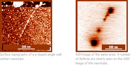
AFM is capable of mapping different electric properties of materials to topography images. These data can be used for analysis of the structure and composition of heterogeneous samples, as well as for quantitative characterization of individual grains or defects on surface.
Fig. 1. Images are courtesy of Sergei V. Kalinin, Marcus Freitag, AT. Johnson, Dawn A. Bonnell, University of Pennsylvania. |
 |
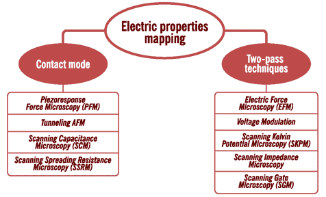
Electric properties of a sample can be mapped using AFM probes with conducting coatings, when AC or DC bias is applied between the AFM tip and the sample. Contact mode or lift mode can be used for this purpose.

Electric Measurements in Contact Mode
A number of specific AFM experiments such as studies of piezoresponse (Piezoresponse Force Microscopy), capacitance (Scanning Capacitance Microscopy) and measurements of DC/AC current (conducting AFM, tunneling AFM, current-sensing AFM, etc) are performed in contact mode AFM.
Contact electric techniques generally require the absence of a gap between the AFM tip and the sample and sufficient area for ohmic or capacitive contact, which is related to higher tip-sample forces and AFM cantilever spring constants (up to 50N/m) than in regular contact mode. Relatively soft (0.03-0.3N/m) conducting AFM cantilevers are optimal for high lateral resolution while AFM cantilevers with a higher spring constant are better for quantitative measurements.
The measured currents can lie in the range of 100fA for Tunneling AFM to 1A for SSRM. However, it is generally not recommended to exceed the 200nA current limit for coated AFM probe tips. The conductive diamond coating of the HQ:DMD series ensures the highest tip lifetime in this demanding application. The Pt coating offers acceptable resistance to wear and electromigration firmness. AFM tip radii of Pt coated AFM probes vary from <40nm for the low-noise HQ:DPE series down to <20nm for the high-resolution HQ:DPER series.
Electric Measurements in Oscillatory Modes
The investigation of electric properties is performed in single-pass or two-pass (lift-mode) techniques. Traditionally, AFM probes of stiffness ~5N/m with conducting coatings are used for lift-mode measurements. In some cases, doping of the Si wafer, which was used for microfabrication of the probes, is sufficient to provide reasonable force response to electrostatic interactions with a sample.
Lift mode measures topography during the first pass and another electric or magnetic property of the sample during the second pass. This minimizes the interference between the two kinds of data. The spring constant and resonance frequency of the AFM cantilever should be chosen to provide stability in tapping mode and high sensitivity to weaker forces on the second pass. In most cases the HQ:NSC18/Pt AFM probes are a good place to start. The Pt coating offers an AFM tip radius of <30nm and good wear-highest resistance.
Among the serious limitations of Electrical Force Microscopy are the sensitivity and signal-to-noise ratio. Enlargement of the AFM probe tip radius can increase the area of electrical interaction and improve these parameters, but this improvement leads to a loss of resolution in both topography and EFM imaging. The HQ:DPE-XSC11 AFM probe consists of a special structure of conductive layers, which provides a more stable electrical signal and less noise with little impact on resolution.
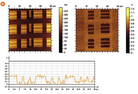
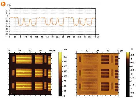
Fig. 2. compares the topography and EFM scans of a semiconductor structure imaged by a standard HQ:NSC14/Pt AFM probe and the new HQ:DPE-XSC11 AFM probe. The signal-to-noise ratio for the scans taken with the HQ:NSC14/Pt is about 3-4, while it is more than 10 for the scans using the DPE AFM probe.
| Fig. 2a. Topography (left) and surface potential (right) images of a Static Random Access Memory(SRAM) structure obtained by single-path Kelvin Force Microscopy. A standard HQ:NSC14/Pt AFM probe with an AFM tip radius of ~25nm has been used. |
 |
| Fig. 2b. Topography (left) and surface potential (right) images of a SRAM structure obtained by single-path Kelvin Force Microscopy. An HQ:DPE AFM probe has been used.” Image courtesy of S. Magonov, Agilent Technologies |
 |
